
[HOWTO] - ATLYS & MicroBlaze
This guide describes the design flow for developing a custom embedded processing system using Xilinx EDK.
The Embedded Development Kit (EDK) is a suite of tools and IP that you can use to design a complete embedded processor system for implementation in a Xilinx FPGA device.
The EDK essentially consists in XPS & SDK.
Xilinx Platform Studio (XPS) is the development environment used for designing the hardware portion of your embedded processor system. You can run XPS in batch mode or using the GUI, which is what we will be demonstrating in this guide.
The Software Development Kit (SDK) is an integrated development environment, complementary to XPS, that is used for C/C++ embedded software application creation and verification.
For other usefull information like as requirements (sw or hw), software platform or else you can refer to reference section.

Here the few and simple steps that we're going to do:
1) Create a new project in XPS;
2) Export the project to SDK;
3) Write a trivial application in C/C++ in a SDK project;
4) Transfer the system and application to Atlys board;
5) Test the system & app.
1) Create a new project in XPS
Set the directory of design and the reference library.
As reference we use the ATLYS BSB 3.6 (AXIS lib).

Select Atlys board after that you have choosen Digilent brand.

Select , with add & remove button, your hardware specification.
You can also manage single block in the dx side of the foam.

The System Assembly View allows you to view and configure system block elements.

MHS file contain the definition of external and internal port.
External definitions coincide with external pinout.
When a PORT is shown inside of a BEGIN/END pair it’s a port on a piece of IP. When you see a PORT at the top of the MHS, it connects the embedded platform to the outside world.

For a design to work in an FPGA, it needs to be converted to a bitstream. This conversion is the following three-step process:
1. XPS generates a netlist that is representative of your embedded hardware platform.
2. The design is implemented (mapped into FPGA logic).
3. The implemented design is converted to the bitstream that can then be downloaded to the FPGA.
When we generate the netlist the XPS
- Reads the design platform configuration MHS file and runs all necessary
design rule checks to validate the correctness of the design.
- Synthesizes the design using Xilinx Synthesis Technology (XST).
- Produces netlist files (with an .ngc extension) for each peripheral, as well
as the overall embedded system.
- Generates Hardware Description Language (HDL) wrapper files for each
peripheral and the overall system. To see the created HDL files, look in
the <project_name>\system\hdl directory.

Generation of bitstream file.
Compiled C code is not part of this bitstream. It is added later in SDK.

2) Export the project to SDK
Created the project and added an embedded processor source, designed your hardware platform in XPS using the Base System Builder, and finally generated a bitstream for the FPGA, now, you will export your hardware platform description to the Software Development Kit (SDK).

When you export your hardware design to SDK, a utility creates , in addition to the XML file, documentation on the software drivers and hardware IP is included so you can access necessary information from within SDK.
When SDK launches automatically, it imports the hardware platform for your design.


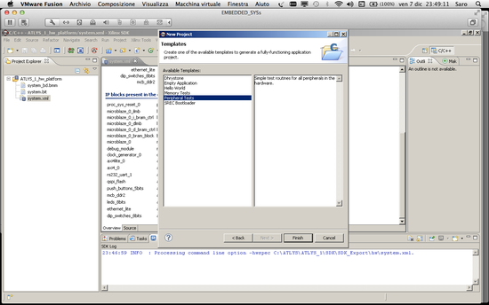
3) Write a trivial application in C/C++ in SDK project
A software project contains one or more source files, along with the necessary header files, to allow compilation and generation of a binary output (.elf) file. A workspace can contain multiple software projects. Each software project must have a corresponding board support package.


SDK examined your hardware specification file (system.xml) and compiled the appropriate libraries corresponding to the components of your hardware platform. You can view the log for this process in the Console view.
You can see lscript.ld, the default linker script that was generated for this project. A linker script is required to specify where your software code is loaded in the hardware system memory.
Double-click the lscript.ld file to view the linker script contents in the text editor.
If you are familiar with the intricacies of linker scripts, you can make changes by selecting Xilinx Tools > Generate Linker Script.
You now have a complete framework for editing, compiling, and building a software project. The next step is debugging.

4) Transfer the system & app to Atlys
You must configure a bitstream that loads a design into the FPGA. In this case, the design is an embedded processor system.

5) Test the system & app
The code you executed in SDK displays test text message in the terminal window to demonstrate how simply software can be executed using SDK.

References:
[16] Xilinx documentation about EDK/SDK