ADDS - Arbitrary Direct Digital Synthesizer
Introduction:
The direct digital synthesizer (DDS) circuit is also known as numerically controlled oscillator (NCO).
The DDS has the following basic blocks:
a phase accumulator;
a phase to amplitude converter (a sine ROM);
a DAC;
a filter.
The phase accumulator consists of a N-bit frequency register which stores a digital phase increment word followed by a N-bit full adder and a phase register.
The read only memory (ROM) is a sine LUT (look-up table), which converts the digital phase information into the values of a sine wave.
The DAC convert digital data to analog.
The filter (conventionally LPF) to cut unwanted armonics and spurs.
Related to the performances and to the problematics for each stage, often, add several blocks like dithering algorithms, modulators, or registers ... or others is nedded for achieved the specifications.
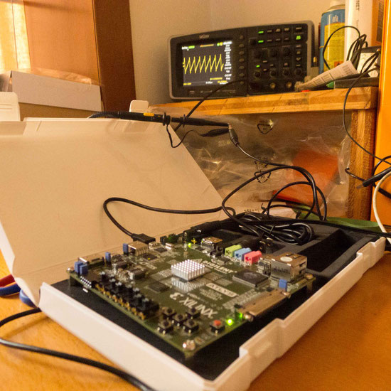
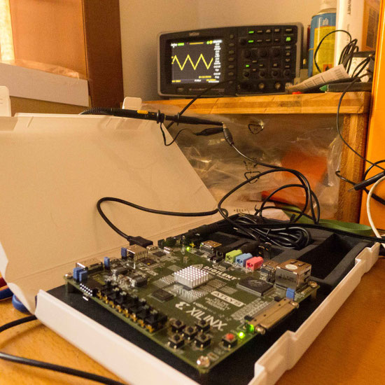
Implementation:
The system implemented actually can generate:
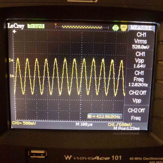
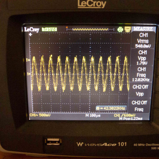
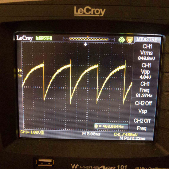
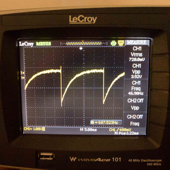
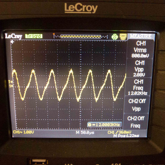
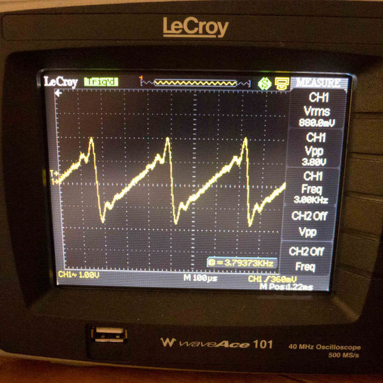
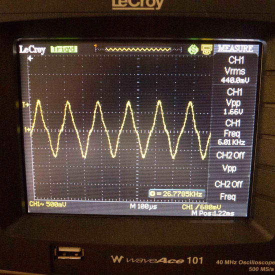
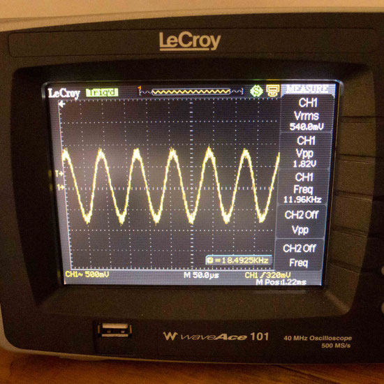
sine waves, triangular waves, saw waves selected by a bus signal (sel). The frequency range is from DC up to 16kHz (this limit is due to Atlys DAC that is part of an audio controller LM4550). The frequency, actually, is selected by a bus signal (word).
The core of the system is the phase accumulator that drive the ROM.
Most of the problems for achieve the specifications are due to this stage, parameters like frequency resolution, max or min frequencies, SNR, spurs generation, speed of the system, power consumption and cost are strongly influeced by its characteristics.
For many questions I chose 31bits as bit depth of accumulator.
The DAC controller (audio!!!) of Atlys works with only 18bits then a bit-shifting operation is required before send data packages to the LM4550 (only for saw and triangular waves).
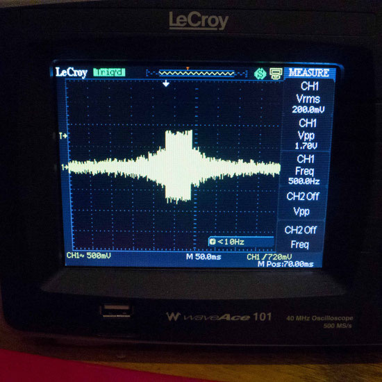
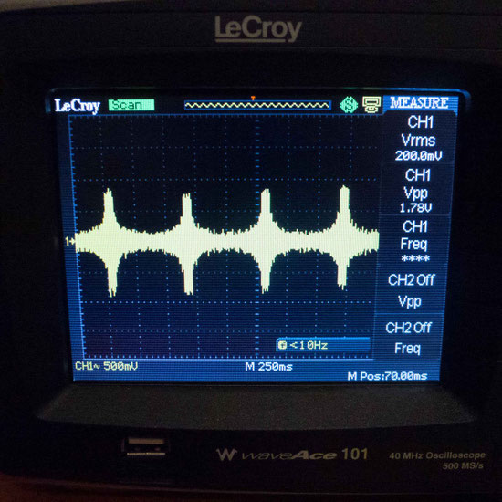
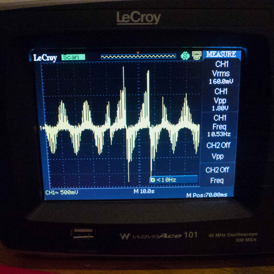
Actualy no filters banks are implemented and this introduces not a few problems as you can see below in disturbs, jitter section.
Results:


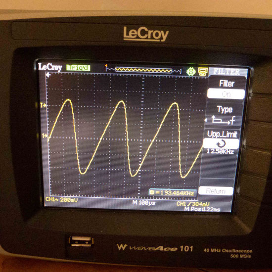
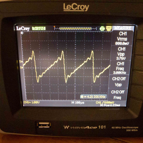
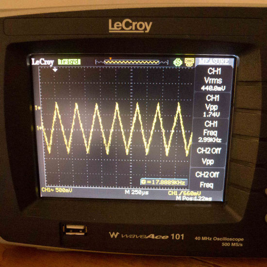
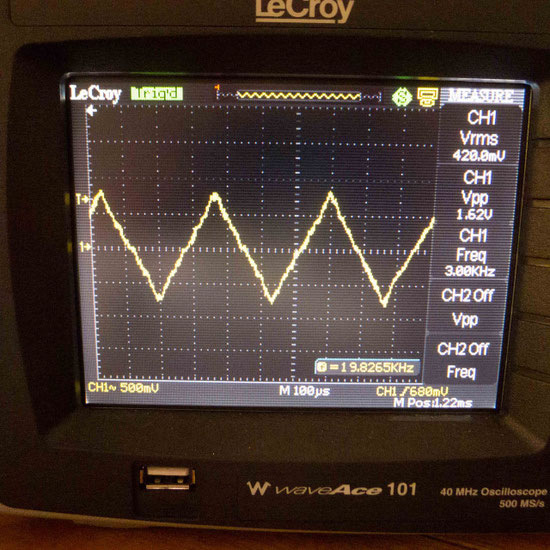
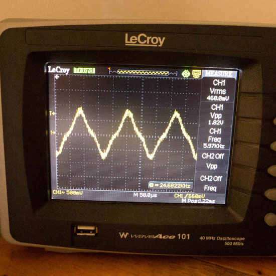
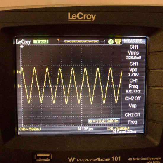
Distrurbs, Spurs, Noises & Jitters:
Next steps:
The next steps are:
- Provide the system of an UART (RX) module that can receive commands from a shell (probably a linux shell) trought USB;
- A FSM is required for manage all modules;
- Implement a AM/FM modulation module;
- Implement a Filter module for prevent the noise and the jitter;
- Use an external DAC instead that LM4550 that is to frequency limitated for all not-audio applications. The Atlys-VHDC output can be used for this purpose.
Upgrades:
2013/02/18:
I have done a set of modules for manage three press buttons and an attenuation module.
Actually the system gained the feature to change the amplitude of the output.
The attenuation work like a programmable division module for the output of the mux.
The next step: write another set of modules for implement the AM modulation.
2013/02/21:
I 've done a new module for make a signed binary division.
2013/02/22:
I completed another set of modules for implement & manage the AM modulation.
In this moment the system use a sw button to drive a mux that select between an AM_counter (a triangular wave) and the old system to change the amplitude of output manually.
The output of this mux drive the divisor of the new signed binary division module.
The system work well, next days I upload the page with a new block diagram and some photos.
2013/02/23:
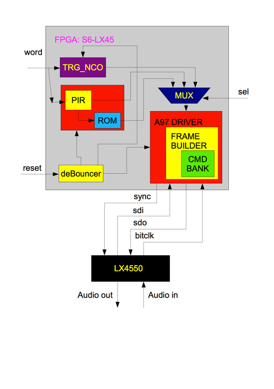
Below the new block diagram.
The new entry:
- the btn_press_counter is a counter incresed/decresed/resetted by three
press button. This counter value have the same size of divisor of
signed_binay_division module.
- The AM_mod_Cnt is another bidirectional counter (act like a triangular
wave). This counter value have the same size of divisor of
signed_binary_division module.
- The signed_binary_division module act the signed division between the
dividend (the out of the mux in which are wired the out of oscillators) and
the divisor (out of AM_mod_Cnt or out of Btn_Press_Counter).