
Howland's Current Pump
It is well known to analog designers that you can use the property of OPamp to implement a high-impedance current pump.
As Robert A. Pease, National Semiconductors expert, remember in his application note AN1515 in Jannuary 29,2008; "the theory is simple. But the pratical problems involved are not so simple or obvious."
The Howland's current pump (HCP), invented by prof. Bradford Howland of MIT in 1962, can put on a current in either direction or AC currents.
The peculiarity is that the feedback from output to both the + and - is at equal strength.

If the node " OUTPUT ", which coincides with the +input of OPamp, is grounded we can see, for ispection, that the " gain " is 1/R1 (the circuit work as a trans-ammettance amplifier) the resistor R2, R3, R4 have no effect (Vin+ voltage active).
When you increase the voltage od -input the gain to the output node (as well know) -R4/R3 * 1/R2. Since the ratio of the resistors is defined to be R1/R2=R3/R4, then the gain is also -1/R1. Therefore the gain is the same but with an opposite sign.
If both Vin+ and Vin- are moved together there is no change of Iout (I of RLOAD).
For the output impedance we can say that if both input signal are grounded, and if output node is lifted up, something has to drive the resistance R1.
As the OPamp's +input is lifted, the -input also rise up, and the output also rises, providing the current through R2 to cancel the flowing through R1.
Brief Analysis:
(VIN- - V-)/R3=(V- -VOPOUT)/R4 (1)
(V+ - VOPOUT)/R2 =(VIN+ - V+)/R1 - IL (2)
Since R1/R2=R3/R4 in particular (R3=R1 & R2=R4) and V+=V-
IL= (VIN+ - VIN-)/R1 (3)
Equation founded say that the output current depend from R1 through the differential voltage applied to the OPamp input.
Now assume that R2=R4 but R1 != R3 (!= -> disequal):
(VIN- - V-)/R3=(V- -VOPOUT)/R2 (4)
(V+ - VOPOUT)/R2 =(VIN+ - V+)/R1 - IL (5)
Therefore since V+ = V- = VL :
(VIN- - VL)/R3=(VIN+ - VL)/R1 - IL then: (6)
IL= 1/R1*[VIN+ - (R1/R3)* VIN-] -VL(R1-R3)/R3R1 (7)
If we put Rs=R3R1/(R3-R1)=R1/tol1 (tol1=R3-R1/R3 relative diff) (8)
we can say that the equivalent source resistance is proportional to R1 and inversely to relative difference calculated respect the other resistor (R3).
From the formulas above we can see that the match of the resistors or better them tollerances are the fundamental requirement that ensure that the output ammettance is low (high impedance).
Mr. Pease in his application note suggests various ways to guarantee this specification:
1. Buy resistors with tighter tolerances - or
2. Sort and match them by pairs. This is cheap and simple
if you only need a small number of well-matched resistors, and you don't want to go out and buy special parts. Just match the R's you have.
3. Add a trim-pot in series with one of the resistors, and add a compensating resistor of about half that size, on the opposite side, to let you trim the
ratio up or down a little. Of course, if any pot can be adjusted, it can also be mis- adjusted...
4. Buy matched sets of tightly-matched resistors. These can be purchased in sets of 4 for a couple dollars, in an SOIC package, such as four 10k resistors matched to 0.1% or even to 0.01% of ratio. These are available with matching".
One of the weaknesses of the Basic HCP is its output capability. Its output node does not normally swing very close to the rail.
Another weakness of the Basic circuit is the inefficiency. If you want to have a gain of (1/100 ohms), with R1 at 100 ohms, the amplifier has to put out a lot of drive, if the load voltage swings a lot. If the load is a low voltage, such as a diode, that may not be so bad. If the load only rises a half volt, only a few mA will be wasted. But if it had to rise 5 volts, that is a lot of power wasted!
If you had to drive a heavy load, you do not have to have equal resistances at R1 and R3. You could have 100 ohms, 100 ohms for R1/R2, and 10k/10k for R3/R4. Then if you want to drive the - input, the input impedance will not be very heavy. However, when you have this imbalance, you must be careful that the amplifier's Ib does not cause a big error, which may be significant if a bipolar input op amp is used.
To avoid these weaknesses of the Basic Howland, the "Improved" Howland generally does solve many of these problems, very well.
The “Improved Howland” Current Pump
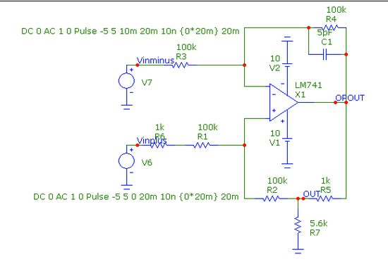
In the improved HCP the gain is set by R5, modified by the ratio of R3/R4 (which is typically 1/1). Therefore you can use low values for R5, and keep all the other resistors high in value, such as 100kΩ or 1 MΩ.
In the "Improved" Howland, note that it is not just the ratio of R1/R2 that must match R3/R4; it is the ratio R1 / (R2 + R5) that must be equal to R3/R4. If you do the intuitive analysis as mentioned above, you can see that if R3 = R4, R2 will normally be (R1 - R5). You could make R1 a little higher, to get the gain to balance out. You could put a 2kΩ pot in series with R1. This "improved" circuit can now force many milliamperes (or as low as microamperes, if you want) into voltages as large as 10 volts, with good efficiency.
We can also notice the presence of a little capacitor, C1, in parallel with R4 for prevent another kind of weakness. This capacitor correct the dynamic aspect of OPamp.
How Pease remember "an operational amplifier can move its output quickly, only if there is a significant Vin transient or Error Voltage (Vε) applied across the inputs". Typically, this can be millivolts, or dozens of millivolts, according to the need for fast output speed.
For Basic HCP (analysis of improved HCP is similar):
The slew rate of Vout, dVout/dt, is equal to: dVout/dt = - 1/(2 π fh) x Vin where (fh) is the Gain Bandwidth Product. Thus, Vε = dVout/dt x 1/(2 π fh)
To analyze this current pump we apply a long, slow ramp at Vx. The dVx/dt is the same as the dV(sum)/dt, and dVout/dt = (R4 + R3)/R3 x dVx/dt.
When we apply the ramp from a negative voltage and Vx just passes 0 volts, with a rate of change equal to dVx/dt, this error voltage Vε will be generated:
When the istantaneous voltage Vx is: Vx
= 0 + dVx/dt, V(sum) = dVx/dt - Vε,
Then Vout has a rate of change, (dVx/dt) (R4 + R3)/R3 and a istantaneous offset of:
- Vε x (R4 + R3)/R3 = -1/(2 π fh) x dVx/dt x ((R4 + R3)/R3)^2. (10)
The current i1 through R1 is zero, since Vx = 0.
The current through R2 is:
i2 = Vout/R2 = - dVx/dt x 1/(2 π fh) x 1/R2 x ((R4 + R3)/R3)^2. (11)
This current acts as a capacitive current, as it is a direct function of dVx/dt. This virtual capacitance is:
C = 1/(2 π fh) x 1/R2 x ((R4 + R3)/R3)^2 (12)
[Cx = 1/(2 π fh) x (1/R13) x R11/(R11 + R12) x [ (R14 + R15)/R14]^2 for improved HCP]. (13)
For a 1 MHz op amp, in a typical application when R1 = R2 = R3 = R4 = 10kΩ, this capacitance will be 200 pf / π , or about 64 pF, (in addition to the actual capacitance at the + input of the operational amplifier). This capacitance is inversely proportional to the gain bandwidth product fh. It gets smaller as a faster amplifier is employed. This capacitance will also be inversely proportional to R2, so for 1 kΩ, it would be 636 pF. For 100 kΩ, it would be just 6.4 pF.
With modern fast op-amps, this capacitance may or may not be a significant factor, but it should be taken into account, depending on the application.
For calculate the dynamic swing we can use the equations (1 & 2) in which R1=R3 and R2=R4:
(VIN- - V-)/R1=(V- -VOPOUT)/R2 (14)
(V+ - VOPOUT)/R2 =(VIN+ - V+)/R1 - IL (15)
Since V+=V-=VL
VL*(1/R1+1/R2)=1/R1*VIN- + VOPOUT/R2=1/R1*VIN+ + VOPOUT/R2 - IL
If the output is limited by Vmax & Vmin:
VLmax = (R1*Vmax+R2*VIN-) / (R1+R2) =
(R1*Vmax + R2*VIN+ - R1R2*IL) / (R1+R2) (16)
VLmin = (R1*Vmin+R2*VIN-) / (R1+R2) =
(R1*Vmin + R2*VIN+ - R1R2*IL) / (R1+R2) (17)
Reference:
[15] Robert A. Pease, National Semiconductors expert, application note
AN1515 in Jannuary 29,2008